


Preheating Kov Screen BGA Rework Tshuab
Nws yog qhov zoo tshaj plaws los hloov cov khoom me me ntawm cov xov tooj smartphones yam tsis muaj kev puas tsuaj rau cov khoom sib txuas thiab lwm yam khoom yas.
Hauj lwm lawm
Preheating Kov Screen BGA Rework Tshuab
1. Khoom nta ntawm Preheating Kov Screen BGA Rework Tshuab
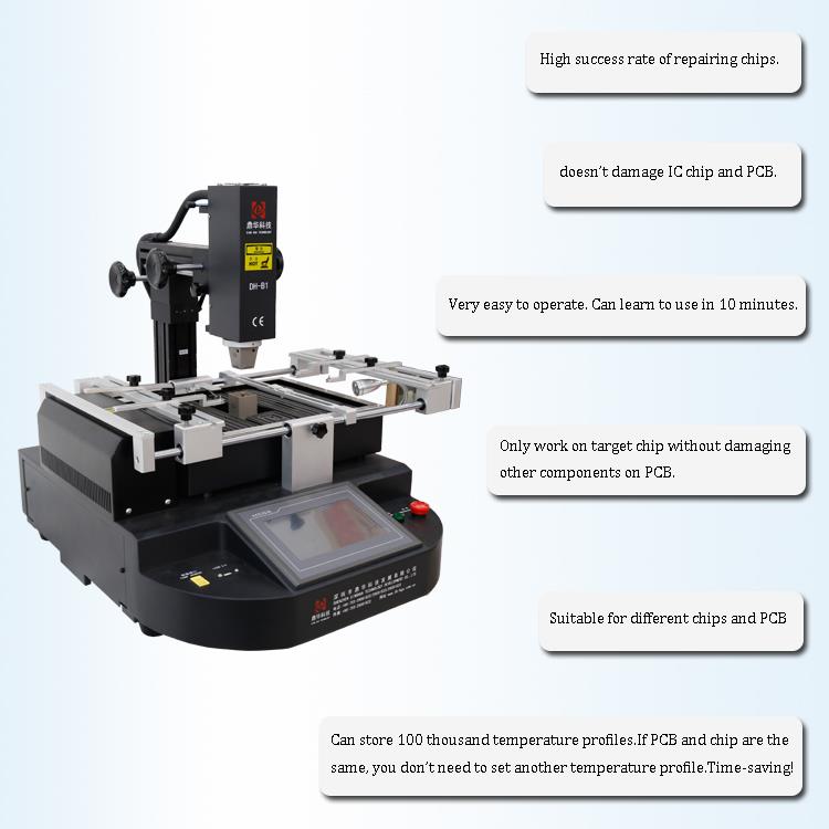
Sab saum toj & hauv qab qhov kub thiab txias qhov kub ntawm nws tus kheej, Lub kiv cua cross-flow txias sai heev los tiv thaiv PCB los ntawm
deformation thaum vuam.
2. Rau cov thermal muaj peev xwm loj ntawm PCB lossis lwm yam kev kub siab thiab cov hlau lead-dawb vuam, txhua yam tuaj yeem ua tau.
tuav tau yooj yim.
3. Kev saib xyuas ua ntej-Heater tiv thaiv tus neeg teb xov tooj los ntawm pib qhov profile thaum lub rhaub tsis tau npaj.
4. Pre-Heater tuaj yeem muab tua lossis muab tso rau hauv SetBack thaum tsis siv qhov system.
Lub tshuab nqus tsev pik tau ua rau hauv theta hloov kho kom yooj yim qhov chaw ntawm cov khoom.
5. Tom qab BGA tshem tawm thiab solder muaj lub suab tswb muaj nuj nqi.
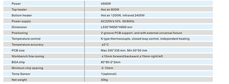
3.Specification ntawm Preheating Kov Screen BGA Rework Tshuab
4.Details ntawm Preheating Kov Screen BGA Rework Tshuab
1. HD kov npo interface;
2.Peb lub tshuab hluav taws xob ywj pheej ( cua kub & infrared );
3. Nqus cwj mem;
4.Led headlamp.


5.Vim li cas thiaj xaiv peb lub Preheating Kov Screen BGA Rework Tshuab?


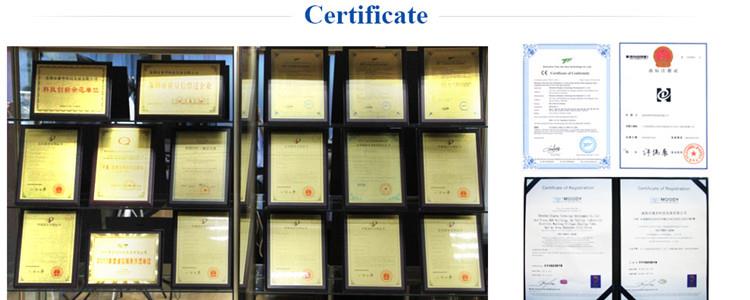
6.Certificate of Preheating Touch Screen BGA Rework Tshuab
7.Packing & Shipping ntawm Preheating Kov Screen BGA Rework Tshuab


8.Kev paub txog
Ob chav sided sib xyaw txheej txheem ntawm SMT
A: incoming inspection => PCB's B-side patch glue => patch => curing => flap => A-side PCB plug => wave soldering =>
cleaning => test =>rov ua dua
Tom qab muab tshuaj txhuam ua ntej, haum rau SMD cov khoom ntau dua li cov khoom sib cais
B: incoming inspection => PCB A-side insert (pinning) => flap => PCB B-side spot adhesive => patch => curing => flap =>
wave soldering => cleaning => Test =>Rework Post-insertion thiab post-fitting, haum rau kev sib cais ntau yam
tshaj SMD cov khoom
C: incoming material inspection => PCB's A surface silk screen solder paste => patch =>
drying => reflow soldering => plug-in, pin bending => flap => PCB B surface patch glue => Patch => Curing => Flap =>
Wave Soldering => Cleaning => Detection =>Rework A nto sib xyaw, B nto mount. ?
D: incoming inspection => PCB's B side spot adhesive => patch => curing => flap =>PCB's Ib sab silk screened solder paste
=> patch => A side reflow => plug-in => B-side wave soldering => cleaning => test =>rework A-sab sib tov, B-sab mounting.
Thawj SMD, reflow, post-fabrication, yoj soldering
E: incoming inspection => PCB side B silk screen solder paste (point mount glue) => patch => drying (curing) => reflow soldering =>
flap => PCB side A silk screen solder paste => Patch => Drying = Reflow soldering 1 (local soldering can be used) => Plug-in =>
Wave soldering 2 (If there are few components, you can use manual soldering) => Cleaning => Test =>Rework A nto mount,
B ntsej muag sib xyaw.


